Device and Circuits: Characterization
Load pull testing
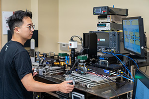
The Wideband Test Facility (WBTF), funded by the Microelectronics Commons program through the Silicon Crossroads Microelectronics Commons Hub, provides capabilities to enable advancements in satellite communications, radar, directed energy, and wireless communications through advanced measurement capabilities for high-frequency transistors, circuits, and antennas. Opened in the summer of 2025, the facility builds on Notre Dame’s existing expertise in high-frequency device and circuit testing to empower and advance the development of state-of-the-art wideband electronic systems and antennas.
Component-level electrical analysis up to 220 GHz
High-frequency device testing assesses the performance of nanometer-scale semiconductor devices, which are essential elements of everything from highend computer chips, to wireless communication systems, to radar and sensing systems. At the WBTF, on-wafer testing of high-speed transistors and circuits can be conducted at frequencies up to 220 Gigahertz (GHz). The ability to test chips at such high frequencies allows for the development of more efficient and reliable device components with unmatched performance.
Notre Dame’s testing capabilities include on-wafer linear network analysis from DC through 220 GHz and passive and hybrid-active load-pull for large-signal device characterization and modeling covering Ka-band (18-40 GHz) and W-band (94 GHz), as well as intermodulation measurements and full noise characterization through these same bands.
This facility also provides full-band noise parameter, intermodulation, and load-pull capabilities covering D-and G-bands (110-170 GHz, 140-220 GHz) for beyond-state-of-the-art wide band gap and ultra-wide band gap transistors, monolithic microwave integrated circuits (MMICs), and systems. Extension to in-fixture and module-level test is also available.
| Key Measurement | Frequencies | Testing Outcome |
| Small-signal characterization | 9 kHz-220 GHz |
• Device speed, frequency response, |
| Large-signal characterization: passive, active, and hybrid-active load pull configurations |
Ka-band: 18-40 GHz |
• Maximum output power, gain • Impedance tuning conditions |
| Noise characterization |
Ka-band: 18-40 GHz |
• Device-level noise contributions to • Impedance tuning conditions to |